Newsletter Subscribe
Enter your email address below and subscribe to our newsletter
Enter your email address below and subscribe to our newsletter
Connecting Circuits, Building Futures.
Semiconductor fabrication is a complex and intricate process that plays a crucial role in the production of various electronic devices that have become an integral part of our daily lives. This article will delve into the processes involved in semiconductor fabrication, ranging from crystal growth to wafer preparation, deposition, lithography, etching, doping, and annealing.
We will explore why semiconductor fabrication is of utmost importance, touching on its role in the production of electronic devices, advancements in technology, economic impact, job creation, medical applications, and environmental benefits. We will discuss the challenges that accompany semiconductor fabrication, including cost, complexity, environmental impact, competition, and technological obsolescence.
Understanding these processes and their significance is essential in comprehending the pivotal role of semiconductor fabrication in today’s technological landscape.
Semiconductor fabrication is the process of creating electronic devices on semiconductor materials such as silicon, involving the manufacturing and assembly of components for CMOS and ICs.
This complex process plays a crucial role in the production of modern electronic devices, like smartphones, computers, and digital cameras. Semiconductor materials possess unique electrical properties that make them ideal for building transistors, diodes, and other electronic components. A range of manufacturing processes, including photolithography, etching, ion implantation, and thermal oxidation, are used to precisely pattern and alter the properties of the semiconductor materials. The intricate design and production of these components require high precision and strict quality control to ensure the reliability and performance of the finished electronic devices.
Semiconductor fabrication encompasses several critical processes, including crystal growth, wafer preparation, deposition, lithography, etching, and doping, each contributing to the creation of intricate semiconductor devices.
Crystal growth forms the foundation of semiconductor fabrication, as it involves the careful formation of a single crystal structure with the desired properties. Wafer preparation then involves slicing these grown crystals into thin wafers and polishing their surfaces to ensure uniformity and cleanliness.
Deposition techniques come into play for adding layers of various materials onto the wafers, while lithography methods use photolithographic processes to transfer patterns onto the wafers. Etching processes then remove materials selectively to form intricate patterns, followed by doping procedures to introduce specific impurities into the semiconductor material to modify its electrical properties.
Crystal growth in semiconductor fabrication involves the precise cultivation of monocrystalline structures on silicon wafers, forming the foundational materials for electronic devices.
This process begins with the preparation of the silicon wafers, which serve as the substrate for crystal growth. These wafers are carefully cleaned and polished to ensure a pristine surface for the subsequent deposition of crystalline layers. The next step involves the introduction of a seed crystal, which serves as a template for the orderly arrangement of atoms during growth.
Under controlled conditions of temperature and pressure, the atoms within the melt align themselves with the crystal structure of the seed, slowly extending the lattice to form a single, uniform crystal. This method of producing monocrystalline structures ensures the absence of grain boundaries and defects, thereby enhancing the electrical properties essential for semiconductor applications.
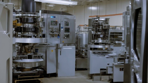
Wafer preparation involves meticulous cleaning and testing procedures in a controlled clean room environment to ensure the removal of impurities and the evaluation of electrical properties before subsequent processing and packaging.
After the initial cleaning process, the wafer undergoes impurity removal steps such as etching or ion implantation to achieve a high level of purity.
Electrical testing is then performed to assess the functionality and integrity of the wafer, ensuring that it meets the specified standards for the intended application.
Once the testing phase is completed, the wafers are carefully packaged to protect them from contamination or damage during storage and transportation, thus safeguarding their quality and performance.
Deposition in semiconductor fabrication involves the controlled addition and removal of thin films to create insulating and conducting layers, contributing to the formation of intricate circuit components.
The process of deposition plays a crucial role in the development of advanced electronic devices. By carefully depositing thin films onto substrates, manufacturers can manipulate the electrical and structural properties of semiconductors, enabling the creation of complex circuitry. At the heart of this process lies the ability to form precise patterns and structures, leveraging the insulating and conducting characteristics of these layers to sculpt the intricate components that define modern electronics.
Lithography is a pivotal technology in semiconductor fabrication, enabling the precise patterning of features on nanometer-scale nodes through techniques such as photolithography and selective etching of oxide layers.
Photolithography, a key process within lithography, involves projecting a pattern onto a photosensitive surface, allowing precise reproduction of intricate designs onto semiconductor wafers. The subsequent etching processes, including wet and dry etching, are vital for removing unwanted material, creating the desired circuit patterns on the silicon substrate.
The impact of lithography extends to the advancement of nanometer-scale nodes, where semiconductor devices have become increasingly complex and integrated. Continued innovation in lithography techniques is crucial for achieving higher levels of miniaturization and performance in modern electronic components.
Etching plays a crucial role in semiconductor fabrication by selectively removing material layers using ions and metal compounds, contributing to the creation of gate dielectrics, spacers, and nanometer-scale features.
Etching starts with the application of a patterned mask, protecting certain areas while exposing others to a chemical or physical etchant. This allows for the precise removal of specific materials without affecting the surrounding areas. Different types of etching, such as wet etching using liquid etchants or dry etching involving plasma, are employed based on the desired outcome.
The patterns created through etching form the foundation for integrated circuits and other semiconductor devices, enabling the precise arrangement of conductive and insulating layers.
Doping is a critical process in semiconductor fabrication, involving the introduction of dopants to modify the electrical properties, junction depths, and charge transport characteristics, influencing device mobility and performance.
This process plays a vital role in tailoring the behavior of semiconductors by significantly altering their conductivity and carrier concentration. By strategically incorporating dopants such as boron, phosphorus, or arsenic into the semiconductor crystal lattice, manufacturers can manipulate the material’s conductivity and voltage properties. This modulation of electrical characteristics forms the basis for the creation of diodes, transistors, and other semiconductor devices essential in modern electronics.
Annealing is a critical step in semiconductor fabrication, involving the controlled application of temperature to repair defects, optimize the crystalline structure, and relieve stress in manufactured devices.
This process is essential as it helps restore the crystal lattice structure of the semiconductor material, which is often disrupted during the manufacturing stages. By subjecting the material to carefully controlled heating and cooling cycles, the internal stresses are minimized, ensuring the performance and reliability of the final semiconductor devices.
Annealing plays a crucial role in reducing the number of defects in the material, thereby enhancing its electrical and mechanical properties. It also aids in optimizing the electrical characteristics of the semiconductor, making it more efficient in its intended application.
Semiconductor fabrication is vital due to its role in producing essential electronic devices, driving technological advancements, and contributing significantly to the global economy.
The process of semiconductor fabrication involves the manufacturing of semiconductor devices that are integral to the functioning of myriad electronic products, such as computers, smartphones, and automotive components. This industry not only shapes the development of cutting-edge technologies but also serves as a cornerstone for economic growth and innovation worldwide.
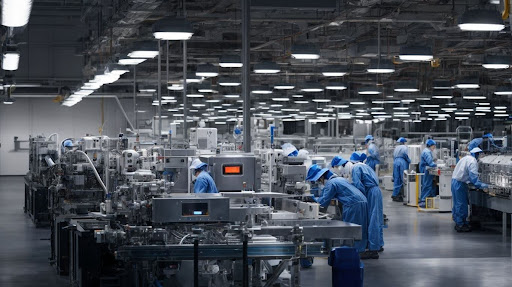
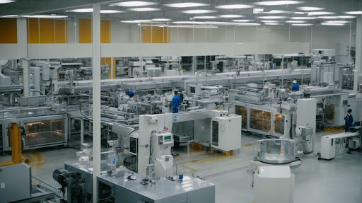
Semiconductor fabrication plays a pivotal role in the mass production of electronic devices, involving precise manufacturing processes, materials testing, and packaging techniques to ensure quality and performance.
The fabrication process typically begins with silicon wafers that undergo a series of intricate steps including photolithography, etching, doping, and thin-film deposition to create integrated circuits. The choice of materials and their properties are rigorously tested to meet the demands of miniaturization and performance.
Packaging considerations are crucial for protecting the delicate semiconductors from environmental factors and mechanical stress, ensuring their reliability and longevity.
Semiconductor fabrication drives continuous advancements in technology, facilitating the development of cutting-edge CMOS, ICs, and lithography techniques for nanometer-scale precision and performance.
These innovations have revolutionized the electronics industry, enabling the production of smaller, faster, and more energy-efficient devices. The development of CMOS (Complementary Metal-Oxide-Semiconductor) technology has been pivotal in achieving high integration density and low power consumption. It has significantly contributed to the miniaturization of electronic components, making portable devices and complex systems such as smartphones, tablets, and computers possible.
The advancement of ICs (Integrated Circuits) has led to remarkable improvements in processing power and functionality. ICs have become the backbone of modern electronic systems, with their compact size and enhanced performance capabilities reshaping various industries, including communication, healthcare, and automotive.
The refinement of lithography techniques plays a crucial role in achieving nanometer-scale precision. This technology has enabled the manufacturing of intricate patterns on semiconductor wafers, allowing for the production of high-performance microchips and semiconductor devices. As a result, technological advancements in lithography have paved the way for enhanced computational capabilities, reduced energy consumption, and expanded applications across diverse fields.
Semiconductor fabrication has a substantial economic impact, driving growth in the industry, creating jobs, and contributing to the stability and innovation of the global economy.
The production of semiconductors is a critical component of numerous industries, including technology, automotive, and healthcare. By enabling the development of advanced electronic devices, this process fuels innovation and progress across various sectors, thereby enhancing productivity and efficiency. Semiconductor fabrication facilities stimulate economic development in the regions where they are established, attracting investments, fostering R&D activities, and generating employment opportunities. This ripple effect extends further, positively influencing the overall economic landscape and promoting sustainable growth.
Semiconductor fabrication significantly contributes to job creation by fostering a robust manufacturing industry and driving technological innovation, thereby enhancing employment opportunities within the global economy.
With the rapid advancement of semiconductor fabrication technologies, the demand for skilled labor in this sector has grown substantially. The expansion of semiconductor fabrication facilities has a cascading effect on job creation, not only within the manufacturing sector but also in supporting industries such as logistics, supply chain management, and research and development. The continuous evolution of semiconductor materials and production processes drives the need for specialized talent, further propelling employment opportunities within the high-tech and engineering fields.
Semiconductor fabrication has diverse medical applications, enabling the development of precise and innovative devices that contribute to technological advancements in healthcare and medical technology.
Through semiconductor fabrication, medical advancements have been realized in various areas such as diagnostic imaging, biosensors, and implantable medical devices. The intricately designed semiconductor devices play a crucial role in improving the accuracy and effectiveness of medical diagnostics and treatment.
The integration of advanced materials and miniaturized components has led to significant innovations in personalized and portable medical technologies.
Semiconductor fabrication offers environmental benefits through the development of cleaner and more efficient manufacturing processes, contributing to sustainable technological advancements and reduced environmental impact.
One of the primary environmental benefits of cleaner semiconductor manufacturing processes is the reduction of hazardous chemical emissions into the atmosphere. By implementing innovative technologies such as green chemistry and energy-efficient equipment, semiconductor fabs can significantly minimize their carbon footprint.
The utilization of renewable energy sources in the production of semiconductors plays a crucial role in enhancing the sustainability of the industry. By investing in solar and wind power, semiconductor manufacturers can substantially decrease their reliance on non-renewable energy, thereby fostering a more environmentally friendly approach to production.
Semiconductor fabrication presents several challenges, including cost constraints, complexity in manufacturing processes, competition within the industry, and the risk of technological obsolescence.
Cost constraints are a fundamental concern as the semiconductor industry demands significant capital investment to build and upgrade fabrication facilities. The complexity in manufacturing processes and the need for cutting-edge technologies add to the overall expenses.
Intense competition within the industry compels manufacturers to continually innovate, optimize production, and manage costs efficiently to stay ahead. The risk of technological obsolescence poses an additional challenge, requiring companies to constantly adapt and invest in R&D to keep up with rapidly evolving technologies.
Cost remains a significant challenge in semiconductor fabrication, impacting manufacturing processes, technology investments, and the overall economic impact of the industry.
Semiconductor fabrication involves intricate and complex processes that necessitate substantial financial investment, from research and development to the actual manufacturing phase. The development and implementation of cutting-edge technologies often require substantial funding, putting a strain on the resources of semiconductor companies.
The challenge of cost extends beyond the initial investment, impacting the operational expenses and competitiveness of manufacturers in the global market. The economic implications of cost in semiconductor fabrication influence the pace of innovation, product pricing, and the industry’s ability to adapt to evolving consumer demands and technological advancements.
The inherent complexity of semiconductor fabrication poses a significant challenge, requiring intricate processes, advanced materials, and cutting-edge technology to achieve desired performance and precision.
One of the key complexities in semiconductor fabrication lies in the intricate processes involved. From lithography to etching, and doping to packaging, each step demands meticulous attention to detail and exacting precision. Advanced materials such as silicon wafers, conductive materials, and insulators play a critical role in the production of semiconductors, adding another layer of complexity to the process.
The technological requirements are constantly evolving, pushing the boundaries of performance and precision. The industry demands state-of-the-art equipment for semiconductor fabrication to keep pace with the escalating need for smaller, faster, and more energy-efficient semiconductor devices.
Addressing the environmental impact of semiconductor fabrication presents a notable challenge, requiring sustainable and eco-friendly processes to minimize ecological footprints and ensure responsible technological development.
The semiconductor industry, while revolutionizing modern technology, has been under increasing scrutiny for its environmental impact. The fabrication process involves numerous chemical compounds, high energy consumption, and water usage, contributing to pollution and resource depletion. It’s imperative for semiconductor manufacturers to prioritize sustainability and eco-friendliness in their operations.
Implementing green semiconductor fabrication practices involves adopting cleaner production methods, recycling and reusing materials, and reducing energy consumption. This would not only mitigate the ecological impact but also contribute to more environmentally responsible technological advancements.
Competition within the semiconductor industry poses a significant challenge, driving the need for continuous innovation, technological advancements, and strategic differentiation to maintain market relevance and leadership.
The semiconductor sector operates in a highly competitive landscape, where staying at the forefront demands a relentless pursuit of cutting-edge technology and pioneering solutions. Without continual innovation and strategic differentiation, companies risk falling behind, as competitors strive to outpace one another through breakthroughs in technology and process optimization. Maintaining a competitive edge necessitates proactive investment in new materials and production techniques, which consolidate a company’s position as an industry leader.
The risk of technological obsolescence presents a notable challenge in semiconductor fabrication, requiring continuous advancements, innovation, and lifecycle management to address the evolving lifespan of electronic devices and technologies.
Semiconductor fabrication is a dynamic field, with the lifespan of electronic devices constantly shifting due to swift technological changes. As a result, the traditional modes of production and design are being challenged by the complexities of obsolescence. Innovations in materials, processes, and equipment are necessary to keep pace with the market demands and to combat the rapid aging of technologies.
Effective lifecycle management is crucial in prolonging the relevance of semiconductor products, necessitating strategic planning and adaptations to avoid premature obsolescence.
Semiconductor fabrication is the process of creating electronic devices on a silicon wafer, which is a crucial component in various modern technologies. It is important because semiconductors are used in almost all electronic devices, including computers, smartphones, and cars, allowing for the creation of smaller, faster, and more efficient devices.
The main processes involved in semiconductor fabrication include photolithography, etching, deposition, and ion implantation. In photolithography, a pattern is transferred onto a silicon wafer using light-sensitive materials. Etching is then used to remove unwanted material, while deposition adds layers of material to create the desired electronic components. Finally, ion implantation is used to alter the electrical properties of the semiconductor.
Semiconductor fabrication has evolved significantly over the years, with advancements in technology leading to smaller and more complex electronic devices. In the early days of semiconductor fabrication, devices were created using a manual process. However, with the development of automation and advanced equipment, the process has become more precise and efficient, allowing for the creation of smaller and more powerful devices.
One of the main challenges in semiconductor fabrication is the need for high levels of cleanliness and precision. Any impurities or defects in the materials or processes can greatly affect the performance of the electronic devices. Additionally, as the demand for smaller and more powerful devices increases, manufacturers are faced with the challenge of creating complex structures on an even smaller scale.
Semiconductor fabrication is used in a wide range of applications, including microprocessors, memory chips, solar cells, and sensors. It is also used in various industries such as telecommunications, healthcare, transportation, and automation. Without semiconductor fabrication, many of the modern technologies we rely on today would not be possible.
Semiconductor fabrication is essential to the advancement of technology. It allows for the creation of smaller, faster, and more efficient electronic devices, which in turn enables the development of new technologies and innovations. With ongoing advancements in semiconductor fabrication, we can expect to see even more groundbreaking technologies in the future.