
Newsletter Subscribe
Enter your email address below and subscribe to our newsletter
Enter your email address below and subscribe to our newsletter
Connecting Circuits, Building Futures.
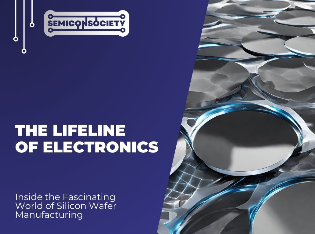
Silicon wafers are a crucial component in various industries, from semiconductor manufacturing to solar cell production.
Learn about the fascinating process of creating silicon wafers, from growing a silicon ingot to polishing the wafers. Explore the different types of silicon wafers and the challenges faced in their manufacturing.
Join us in discussing the future of silicon wafer production and its impact on various industries.
Silicon wafers are thin slices of high-purity silicon used in various industries.The manufacturing process involves growing, slicing, polishing, cleaning, and inspecting the wafers.The future of silicon wafer manufacturing includes advancements in technology and the potential use of alternative materials.
A silicon wafer is a crucial component in semiconductor manufacturing, utilized for the production of electronic devices through a sophisticated process involving crystal growing.
The silicon wafer serves as the foundation upon which microchips and other electronic components are built, making it an essential element in technological advancements. Companies like Okmetic specialize in producing high-quality wafers that meet stringent industry standards for cutting-edge devices. Through advanced technology and precise manufacturing processes, these wafers provide the perfect substrate for creating intricate circuitry essential for modern electronics. The purity and uniformity of the silicon wafer are crucial in ensuring optimal performance and reliability in electronic products.
.jpg)
Silicon wafers are made by first growing a silicon ingot through processes like the Czochralski method, followed by slicing the ingot into thin wafers and polishing them using techniques such as the CMP process.
During the crystal growth stage, the silicon ingot is carefully formed from a molten silicon material, allowing for a highly pure structure vital for semiconductor manufacturing.
Next, the ingot undergoes precise slicing, where diamond or wire saws are used to cut it into wafer-thin pieces, ensuring uniform thickness for optimal performance in electronic devices.
The final step involves wafer polishing, a critical process that utilizes the CMP technique to create a smooth, defect-free surface essential for semiconductor integration into various technological applications.
Growing a silicon ingot involves the meticulous process of crystal growth, where a pure silicon crystal is formed to serve as the foundation for semiconductor and compound semiconductor production.
During the crystal growth process, silicon ingots are typically produced using the Czochralski method, where a seed crystal is immersed in molten silicon and slowly withdrawn while rotating.
This method allows for the controlled growth of a cylindrical silicon crystal with high purity levels, crucial for the successful fabrication of electronic devices.
Impurities in the silicon can severely affect the performance of the final semiconductor product; thus, stringent purity requirements are maintained throughout the ingot growth phase.
The resulting silicon ingot serves as the raw material for slicing into wafers that undergo further processing to create integrated circuits and other semiconductor components.
Slicing the silicon ingot into wafers involves precision cutting techniques to create thin discs of silicon material that are essential for producing electrical components and semiconductor devices.
Regarding the slicing process, precision cutting techniques play a crucial role in ensuring the uniformity and quality of the resulting wafers. Manufacturers utilize advanced machinery and tools to achieve the required thickness and dimensions with utmost accuracy. The material considerations are also significant in this process, as the choice of cutting tools and methods can impact the efficiency and cost-effectiveness of production. These finely sliced wafers are utilized in various electrical applications, where their purity and flatness are critical for optimal device performance.
Polishing silicon wafers involves utilizing advanced techniques like the CMP process to achieve the smooth surfaces necessary for optimal performance in electronic devices and technology applications.
The Chemical Mechanical Planarization (CMP) process is a critical part of wafer polishing, wherein a combination of chemical and mechanical forces is used to remove imperfections and create a flawless surface finish. Surface quality requirements for polished wafers are stringent, with nanoscale deviations impacting the functionality and reliability of microelectronic components.
Polished wafers play a crucial role in electronic device manufacturing, as they serve as the foundation for the production of semiconductors and integrated circuits. The accuracy and precision of the polishing process directly affect the performance and efficiency of the final devices, making it a key factor in ensuring product quality and consistency.
After polishing, silicon wafers undergo meticulous cleaning and inspection processes to ensure the highest levels of purity and quality, critical for their application in electrical components and semiconductor manufacturing.
During the cleaning phase, the wafers are typically subjected to various chemical baths and ultrapure water rinses to remove any residues or contaminants that could impact their performance.
Particle size and concentration are closely monitored to meet stringent ISO standards, ensuring the wafers are free from impurities. Quality control measures involve sophisticated automated systems that detect any defects or irregularities on the surface, guaranteeing the integrity of the wafers. These thorough procedures are essential in maintaining the reliability and performance of silicon wafers in electronic devices.
.jpg)
Silicon wafers find applications in diverse fields such as semiconductor manufacturing for ICs, production of MEMS devices, and the manufacturing of optical components.
In semiconductor manufacturing, silicon wafers serve as the foundation for integrated circuits, essential components of electronic devices. These wafers undergo intricate processes to create multiple layers of circuit patterns, enabling the functionality of devices like smartphones, laptops, and other cutting-edge technology.
On the other hand, in MEMS device production, silicons wafers are utilized to manufacture tiny mechanical and electronic devices, enabling advancements in sensors, actuators, and other miniaturized systems. The precise properties of silicon make it an ideal material for creating intricate and high-performance MEMS devices.
In the manufacturing of optical components, silicon wafers play a crucial role in producing lenses, mirrors, and other components used in various optical systems. The customizable nature of silicon wafers allows for the fabrication of precise and sophisticated optical elements to meet the diverse needs of industries such as telecommunications, medical devices, and scientific instrumentation.
In semiconductor manufacturing, silicon wafers serve as the foundation for producing integrated circuits (ICs) and other electronic components using high-purity electronic grade silicon.
Silicon wafers are crucial in the production process due to their exceptional electrical properties and the ability to exhibit consistent performance across various semiconductor devices. The purity of silicon wafers is paramount as any impurities can significantly impact the functionality and reliability of the final ICs.
Electronic grade silicon is specifically refined to meet stringent quality standards, ensuring that the wafers used in IC fabrication are free from contaminants that could hinder performance.
Silicon wafers are essential in solar cell production, where they facilitate the creation of efficient photovoltaic cells through the integration of compound semiconductors with specific band gap properties.
These wafers serve as the foundation for solar cells by providing a sturdy platform for the deposition of semiconductor materials crucial for converting sunlight into electricity. The composition and purity of silicon wafers significantly impact the efficiency and durability of the final photovoltaic device. The ability to engineer band gaps tailored to harness specific wavelengths of light is a key advantage of utilizing silicon wafers in solar cell design.
MEMS devices utilize silicon wafers as a substrate for creating miniature electronic components using elemental semiconductors, often fabricated through precise crystal growth methods like crystal pulling.
Silicon wafers serve as the foundational platform on which these intricate MEMS devices are built. Crystal growth techniques such as crystal pulling are crucial in achieving the desired properties for the semiconductor components, ensuring reliability and performance. These wafers undergo meticulous processes to define patterns and structures at the microscale level, enabling the integration of sensors, actuators, and other functionalities on a single chip.
Silicon wafers play a crucial role in the production of optical components, where they undergo processes like Float Zone refining to achieve the precise characteristics required for optical applications.
These wafers are at the heart of creating sophisticated optical devices due to their exceptional purity and uniformity. Through techniques like Float Zone refining, impurities are meticulously removed, ensuring that wafers exhibit minimal defects. The properties of silicon wafers such as high refractive index, low absorption coefficient, and excellent mechanical strength make them perfect for optical applications. In the creation of high-quality optical components, the use of silicon wafers provides a reliable foundation, allowing for precise fabrication and optimal performance.
.jpg)
Various types of silicon wafers include monocrystalline silicon wafers, polycrystalline silicon wafers, epitaxial silicon wafers, and SOI wafers, each designed for specific applications in the semiconductor industry.
Monocrystalline silicon wafers are known for their high purity and uniform crystal structure, making them ideal for high-performance integrated circuits and photovoltaic applications.
Polycrystalline silicon wafers, on the other hand, are more cost-effective and commonly used in memory chips and consumer electronics.
Epitaxial silicon wafers are created through a process that allows for precise layering of additional semiconductor materials, often used in advanced transistors.
SOI wafers, or Silicon-on-Insulator wafers, offer improved insulation and reduced power consumption, making them suitable for RF and power devices.
Monocrystalline silicon wafers are known for their uniform crystal structure, making them ideal for semiconductor applications requiring materials with a direct band gap for efficient electronic performance.
These wafers exhibit superior electron mobility due to the absence of grain boundaries, allowing for faster electron movement within the material.
Their high purity levels result in exceptional electrical conductivity, vital for high-performance semiconductor devices.
The single crystal structure of monocrystalline silicon wafers ensures precise control over the orientation of atoms, enhancing the overall functionality of the electronic components produced.
Polycrystalline silicon wafers are characterized by multiple crystal domains, making them cost-effective alternatives for semiconductor applications where material uniformity may be less critical.
These wafers are composed of numerous small silicon crystals, each with its unique orientation, as opposed to the single crystal structure found in monocrystalline wafers. Due to their lower production costs resulting from the manufacturing process, which involves melting and solidifying chunks of silicon, polycrystalline silicon wafers have become popular in the semiconductor industry for certain applications.
Epitaxial silicon wafers are engineered to enhance the electrical properties of silicon substrates, making them ideal for advanced semiconductor technologies requiring precise crystal structures and conductivity.
By depositing a thin layer of silicon on the existing wafer, epitaxial silicon wafers enhance the material’s conductivity and crystal quality. This process optimizes the structural integrity and performance of semiconductor devices, leading to improved efficiency and reliability in electronic applications. The controlled growth of silicon atoms during epitaxial deposition ensures a uniform crystal lattice structure, reducing defects and impurities that can hinder device performance.
SOI wafers feature a thin layer of silicon on an insulating substrate, offering enhanced insulation and reduced power consumption in electronic devices, especially beneficial for advanced compound semiconductor applications.
By incorporating SOI wafers into electronic technologies, manufacturers are able to achieve superior power efficiency due to the reduced parasitic capacitance and improved heat dissipation afforded by the insulating properties of these wafers.
Moreover, SOI wafers play a pivotal role in enabling the development of cutting-edge compound semiconductor innovations, as they provide a stable platform for integrating multiple materials with distinct electrical properties, leading to enhanced device performance and reliability.
Silicon wafer manufacturing faces challenges related to maintaining high levels of purity and uniformity, reducing production costs, and enhancing efficiency in the manufacturing processes.
One of the major hurdles in achieving high purity standards in silicon wafer production is the presence of impurities that can negatively impact the performance of electronic devices. Manufacturers must carefully control the manufacturing environment to prevent contamination during the production process.
Regarding ensuring uniformity in silicon wafer quality, manufacturers need to invest in advanced technologies and precision tools to control the thickness and surface characteristics of each wafer. Consistent quality across all wafers is crucial to meet the stringent requirements of the semiconductor industry.
To address cost-saving initiatives, manufacturers are constantly seeking ways to optimize their production processes, minimize waste, and increase yield. Implementing innovative techniques such as automated monitoring systems and predictive maintenance can help reduce production costs without compromising quality standards.
Enhancing efficiency in silicon wafer manufacturing involves streamlining production workflows, maximizing equipment utilization, and adopting lean manufacturing principles. By improving production efficiency, manufacturers can increase output capacity and meet the growing demand for high-quality silicon wafers in the semiconductor market.
Ensuring the purity and uniformity of silicon wafers is critical in semiconductor manufacturing to guarantee consistent crystal properties and electrical performance in the final electronic devices.
Purity holds immense importance in silicon wafer production as any impurities can lead to defects in the crystal structure, affecting the conductivity and reliability of electronic components.
Cost reduction measures in silicon wafer manufacturing focus on optimizing production technologies, sourcing cost-effective materials, and streamlining processes to enhance efficiency and competitiveness in the market.
In the dynamic landscape of silicon wafer manufacturing, companies are constantly seeking innovative ways to cut costs without compromising on quality. One of the key strategies involves leveraging technology enhancements to automate and accelerate production processes, thereby reducing labor costs and minimizing errors. By integrating advanced machinery and robotics, manufacturers can achieve higher precision and yield rates, leading to significant savings in the long run.
Careful consideration of material selection criteria plays a crucial role in cost reduction. Opting for high-quality yet affordable raw materials, such as silicon ingots with optimal purity levels, can lead to improved product performance and longevity. This strategic approach not only lowers manufacturing expenses but also enhances the overall reliability and functionality of the end products.
Plus technological advancements and material choices, continuous process improvements are essential for driving efficiency in silicon wafer production. Implementing lean manufacturing principles, identifying bottlenecks, and fine-tuning workflow sequences can streamline operations and minimize wastage, resulting in cost savings and accelerated time-to-market. By fostering a culture of continuous improvement and innovation, manufacturers can stay ahead of the competition and thrive in a demanding industry.
Enhancing efficiency in silicon wafer manufacturing involves refining production processes, adopting advanced technologies, and implementing quality control measures to optimize resource utilization and output quality.
One of the key strategies for improving efficiency in silicon wafer manufacturing is to streamline the workflow by identifying bottlenecks and implementing solutions to smooth out the production process. This could involve reorganizing the layout of the manufacturing floor to minimize material handling time and reduce idle equipment.
Process enhancements such as automation can also play a crucial role in improving efficiency by reducing human error and speeding up repetitive tasks. Investing in the latest technological innovations such as AI-driven predictive maintenance and real-time monitoring systems can significantly boost overall productivity.
.jpg)
The future of silicon wafer manufacturing is poised for advancements in production technology, a shift towards alternative materials, and transformative impacts on industries relying on silicon wafers for electronic applications.
One of the major trends in silicon wafer manufacturing is the increasing focus on developing larger and thinner wafers to improve efficiency and reduce costs. This move towards larger wafers, such as 450mm, allows for more chips per wafer, enhancing productivity in semiconductor fabrication processes. There is a rising interest in utilizing new materials like gallium nitride (GaN) and silicon carbide (SiC) due to their superior performance characteristics compared to traditional silicon wafers.
Anticipated advancements in wafer production technology are set to revolutionize silicon wafer manufacturing, enabling more efficient and precise fabrication of electronic and compound semiconductor devices.
These technological innovations not only promise increased productivity and cost-effectiveness but also pave the way for the development of smaller, faster, and more energy-efficient devices.
Enhanced manufacturing processes like advanced lithography techniques and precise crystal growth methodologies are reshaping the landscape of the semiconductor industry, allowing for the production of wafers with higher yields and superior uniformity.
The integration of automation and smart manufacturing technologies accelerates the production cycle while maintaining stringent quality standards, catering to the escalating demand for high-performance electronic components.
An industry-wide shift towards alternative materials poses a transformative challenge and opportunity for silicon wafer manufacturing, particularly in exploring novel compound and elemental semiconductors for future electronic applications.
This trend reflects the industry’s commitment to enhancing performance and energy efficiency through material diversification.
The adoption of compound semiconductors like gallium nitride or indium phosphide offers higher electron mobility compared to traditional silicon, enabling more compact and powerful devices.
Similarly, elemental semiconductors such as diamond or germanium show promise for specialized applications that demand unique material properties.
Challenges like production scalability, cost-effectiveness, and integration complexity need addressing for widespread commercial adoption.
Embracing alternative materials signifies a pivotal step towards pushing the boundaries of semiconductor innovation and meeting the evolving demands of modern technology.”
The evolution of silicon wafer manufacturing will have a profound impact on industries reliant on electronic technologies, driving innovations in crystal growth methods, electronic device production, and technological applications.
Technological advancements in silicon wafer manufacturing are revolutionizing the landscape of electronic industry verticals. With the integration of cutting-edge processes, like advanced crystal growth techniques, the efficiency and performance of electronic devices are being elevated to unprecedented levels. This shift towards more sophisticated manufacturing practices is not only enhancing the quality of electronic components, but also paving the way for groundbreaking applications in various sectors. The continuous refinement of silicon wafer production is ushering in a new era of possibilities in electronic manufacturing and technological advancements.https://www.youtube.com/embed/EFGom2z4mlQ
Silicon wafer manufacturing is the process of creating silicon wafers, which are thin slices of silicon used as the base material for electronic components such as microchips and solar cells.
Silicon wafers are made through a process called Czochralski pulling, where molten silicon is pulled upwards and cooled to form a cylinder. The cylinder is then sliced into thin wafers using a diamond saw.
There are three main types of silicon wafers: single-crystal, polycrystalline, and amorphous. Single crystal wafers are the most expensive and highest quality, while polycrystalline and amorphous wafers are lower in cost and quality.
Silicon wafer manufacturing is crucial in the production of electronic devices, as silicon wafers serve as the base material for integrated circuits and other electronic components.
The standard size for a silicon wafer is 300mm in diameter, or about 12 inches. However, smaller wafers ranging from 100mm to 200mm are also commonly used in the production of microchips.
One of the main challenges in silicon wafer manufacturing is maintaining a high level of purity in the silicon material, as even small impurities can affect the performance of electronic devices. Another challenge is minimizing defects and imperfections during the manufacturing process.