Newsletter Subscribe
Enter your email address below and subscribe to our newsletter
Enter your email address below and subscribe to our newsletter
Connecting Circuits, Building Futures.
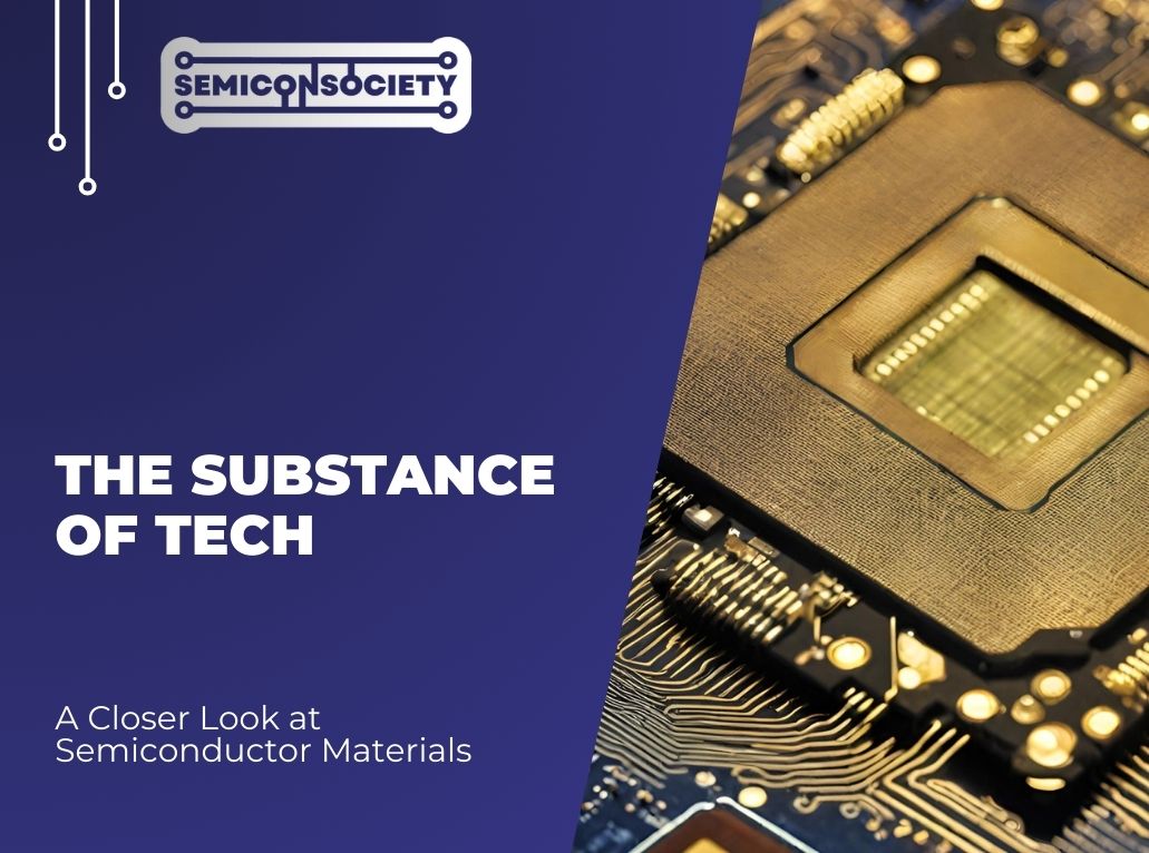

Semiconductor materials are the unsung heroes of modern technology, playing a crucial role in the devices we use every day. In this article, we will explore the different types of semiconductor materials, their properties, and how they are used in various technological applications.
We will also delve into the methods used to manufacture semiconductor materials and discuss the safety precautions that must be taken when working with them. We will take a look at the future of semiconductor materials and the exciting innovations on the horizon.
Join us as we uncover the substance of tech with a closer look at semiconductor materials.
.jpg)
Semiconductor materials play a pivotal role in the electronics industry, with silicon being one of the most commonly used elements for this purpose. Their discovery can be traced back to the work of scientists like Jöns Jacob Berzelius.
The properties of semiconductor materials allow them to conduct electricity under certain conditions, making them essential for creating electronic devices such as transistors, diodes, and integrated circuits. Silicon, in particular, is favored due to its abundance, cost-effectiveness, and stable chemical properties.
The versatility of silicon enables it to be easily processed into various forms, making it suitable for a wide range of applications in electronics. Its use has revolutionized the industry, paving the way for advancements in computing, telecommunications, and beyond.
Jöns Jacob Berzelius, a prominent figure in the history of chemistry, made significant contributions to the study of silicon and other elements, laying the foundation for our understanding of semiconductor materials and their impact on modern technology.
Semiconductor materials encompass a diverse range of compounds, including silicon dioxide, silicon carbide, and gallium nitride, each offering distinct properties and applications.
Silicon dioxide, commonly known as silica, is widely used in the manufacturing of integrated circuits and optical fibers due to its excellent insulating properties.
On the other hand, silicon carbide is valued for its high thermal conductivity and is commonly utilized in high-power electronics and automotive components.
Gallium nitride is prized for its wide bandgap, making it ideal for applications in LEDs, RF amplifiers, and power electronics, especially in the aerospace and defense sectors.
Semiconductor materials possess specific properties that make them ideal for electronic applications, such as their ability to conduct electricity under certain conditions and their sensitivity to external factors.
One of the key properties of semiconductor materials is their bandgap, which determines the energy required for the material to transition from an insulating state to a conducting state. This property plays a crucial role in defining the efficiency and speed of electronic devices.
The process of doping allows for the controlled introduction of impurities into the semiconductor material, altering its conductivity and other electrical characteristics. These properties collectively influence the behavior of semiconductors in electronic devices, making them essential components in modern technology.
.jpg)
Semiconductor materials are integral to modern technology, powering devices such as the Intel 4004 microprocessor and contributing to innovations from companies like Samsung Corporation.
These materials play a crucial role in electronic devices due to their unique properties, such as conductivity control through doping.
For instance, microprocessors rely on semiconductor materials to execute calculations swiftly and efficiently. Memory chips, another vital component, utilize these materials to store data in electronic devices.
Industry giants like Intel and Samsung continually push the boundaries of innovation in semiconductor technology, leading to advancements in consumer electronics, telecommunications, and various other industries.
Semiconductor materials find versatile applications across various industries, driving innovations in electronics, telecommunications, and beyond, as highlighted by the Semiconductor Industry Association (SIA).
The widespread use of semiconductor materials is evident in the consumer electronics sector, where they power devices such as smartphones, laptops, and TVs. These materials are essential for the smooth functioning of digital gadgets and play a crucial role in enhancing user experiences.
In the telecommunications infrastructure, semiconductor materials are instrumental in enabling the seamless transmission of data across networks, supporting the growth and efficiency of communication systems worldwide. From fiber optics to satellite communications, these materials form the backbone of modern telecommunication technologies.
Semiconductor materials are at the forefront of emerging technologies like artificial intelligence, blockchain, and Internet of Things (IoT), where their unique properties are leveraged to build advanced systems that drive the next wave of innovation and connectivity.
Utilizing semiconductor materials in technology offers numerous advantages, such as enhanced processing speeds, reduced power consumption, and increased device miniaturization, exemplified by innovations from industry giants like Intel Corporation.
Integrating these advanced materials into electronic components has proven crucial for pushing the boundaries of performance and efficiency in modern devices. Semiconductors facilitate faster data processing, enabling seamless multitasking and smoother user experiences. Their use results in significant energy savings, contributing to the overall sustainability of electronic products. The ability to miniaturize devices through semiconductor technology has led to the development of sleek, powerful gadgets that enhance convenience and portability for users.
.jpg)
Manufacturing semiconductor materials involves specialized processes like the Czochralski Method, Float-Zone Method, and Epitaxial Growth Method, each tailored to produce materials with specific properties and purity levels.
These methodologies play a critical role in the production of semiconductors.
The Czochralski Method is a well-established technique for growing single crystals of semiconductor materials, involving the controlled solidification of a molten material to create high-quality ingots used in various electronic applications.
This method was developed by Polish scientist Jan Czochralski in 1916 and has since become a fundamental process in the semiconductor industry. The steps of the Czochralski Method consist of melting the semiconductor material in a high-temperature crucible, dipping a seed crystal into the molten material and slowly pulling it out while rotating, allowing a single-crystal structure to form along the seed crystal’s orientation.
One of the main advantages of the Czochralski Method is its ability to produce large, single-crystal structures with minimal defects, making it ideal for manufacturing silicon wafers used in integrated circuits and other electronic devices. The controlled growth process results in crystals with uniform properties, crucial for achieving high performance and reliability in semiconductor components.
The Float-Zone Method is a precise manufacturing process used to produce ultra-pure semiconductor materials, involving the controlled melting and solidification of a material to eliminate impurities and defects, resulting in high-quality crystals.
This method is highly esteemed due to its capability to achieve extremely high purity levels, surpassing other techniques. Notably, the Float-Zone Method ensures the crystals exhibit superior homogeneity and low oxygen content, making them ideal for applications in advanced semiconductor devices. Industries reliant on these high-quality materials include electronics, photovoltaics, and telecommunications, where precision and performance are paramount. The unique advantage of Float-Zone Method lies in its ability to produce single crystals of unmatched purity and structural perfection, elevating the quality standards in semiconductor production.
The Epitaxial Growth Method is a critical process in semiconductor manufacturing that involves depositing single-crystal layers on a substrate to create complex semiconductor structures with precise properties and functionalities.
Utilized extensively in the semiconductor industry, this method plays a pivotal role in the production of a wide range of electronic devices. By controlling the growth of these single-crystal layers, manufacturers can customize the structural and electrical properties of the resulting materials, enabling the development of cutting-edge technologies. Epitaxial growth is particularly crucial in thin-film deposition processes, where it allows for the creation of ultra-thin layers with exceptional uniformity and purity.
In device fabrication, this method ensures the precise formation of semiconductor components, enhancing the performance and reliability of integrated circuits. The ability to achieve epitaxial growth at the atomic level contributes to the production of advanced microelectronic devices with superior functionality and efficiency.
.jpg)
Working with semiconductor materials requires adherence to stringent safety protocols due to potential health hazards associated with exposure, necessitating the use of protective equipment and proper ventilation in handling these substances.
Safety measures are crucial to mitigate the risks involved in handling semiconductor materials. To protect against toxicity risks, it is imperative to wear appropriate personal protective equipment, including gloves, goggles, and respiratory protection. Minimizing chemical exposure can be achieved through proper storage and handling procedures, such as using designated storage areas and implementing spill containment measures.
Preventing contamination is also essential in semiconductor work environments to maintain product integrity and prevent cross-contamination. This involves following strict cleanliness protocols, including regular cleaning of work surfaces and equipment.
Safety training and compliance with safety protocols are paramount to ensure the well-being of personnel working with semiconductor materials.
Semiconductor materials pose potential health hazards, including risks of toxicity, chemical exposure, and respiratory ailments, as highlighted by researchers like Morris Tanenbaum who have studied the effects of these substances on human health.
Over the past few decades, the rapid growth of the semiconductor industry has brought increased concerns regarding the health implications associated with the production and use of these materials.
Studies have shown that exposure to certain semiconductor substances can lead to skin irritation, eye damage, and even neurological issues in individuals. The long-term effects of continuous exposure to these materials are still being researched to understand the full extent of potential health risks.
It is crucial for industries and authorities to implement stringent safety measures to mitigate the health hazards posed by semiconductor materials for the well-being of workers and the environment.
Minimizing exposure to semiconductor materials requires the implementation of safety protocols, including the use of personal protective equipment, proper ventilation systems, and adherence to established handling guidelines to mitigate risks effectively.
Protective measures such as wearing appropriate gloves, goggles, and lab coats are crucial in preventing direct contact with hazardous materials. Ensuring adequate ventilation through the use of fume hoods and exhaust systems helps in reducing airborne particles and fumes.
Implementing strict cleaning routines for workstations and tools also plays a significant role in minimizing the spread of contaminants. Maintaining a clutter-free work environment further enhances safety by reducing the risk of accidental exposure.
Regular training sessions on handling procedures and emergency protocols are vital to educate personnel about the potential hazards and proper safety practices.
The future of semiconductor materials in technology promises continued innovation and advancement, with companies like Broadcom Inc. leading the charge in developing cutting-edge materials and technologies that redefine the industry landscape.
With advancements in areas such as nanotechnology and quantum computing, semiconductor materials are poised to revolutionize various sectors, from healthcare to automotive. Materials like gallium nitride and silicon carbide are garnering attention for their superior properties, offering enhanced efficiency and performance in electronic devices. Researchers are exploring novel applications of these materials, paving the way for smaller, faster, and more energy-efficient technologies. Industry giants are investing heavily in R&D to stay ahead in the competitive market, driving a wave of innovation that is set to reshape the technological landscape in the coming years.
Ongoing innovations in semiconductor materials are driving breakthroughs in diverse applications, with companies like Texas Instruments Incorporated at the forefront of developing cutting-edge materials that enhance device performance and efficiency.
One of the key arenas where these advancements are making significant strides is in the realm of nanotechnology. Nanoscale materials and structures are revolutionizing the semiconductor industry, enabling the creation of smaller, more powerful devices with enhanced functionalities. Texas Instruments has been actively involved in leveraging nanomaterials to push the boundaries of what is possible in electronic components.
Semiconductor materials are substances that have properties between those of a conductor and an insulator. They are used in the production of electronic devices and are the foundation of modern technology.
Unlike conductors, which allow the flow of electricity, and insulators, which block it, semiconductor materials have a varying level of conductivity depending on external factors such as heat, light, or voltage.
Silicon, germanium, and gallium arsenide are some of the most commonly used semiconductor materials in the production of electronic devices such as transistors, diodes, and integrated circuits.
Semiconductor materials are typically made through a process called doping, where impurities are intentionally added to alter their conductivity. This process allows for the production of different types of semiconductors with specific properties.
Semiconductor materials are essential to modern technology because of their ability to control and manipulate the flow of electricity. They are the foundation of electronic devices and have revolutionized the way we communicate, work, and live.
As technology advances, the demand for more efficient, smaller, and faster electronic devices grows. This drives the development of new semiconductor materials and the improvement of existing ones, ensuring the ongoing progress of technology.